Two and a Half Times Part 1B bis
This blog post is different from all the others in that I have chosen a different mechanism
to present it to you. Blog Posts up to this one have been presented to you in a way that has
utilized all the features and been subjected to all the short comings of my Wordpress
installation. Wordpress has been interesting to use, and I have been using it for some time
now. My use of it has been for a tool for presenting my blog, and not as a focus for enthusiasm
in itself. I must thus be considered to be a neophyte user. I got it to do what I wanted, and
(up until now) have left it at that.
Wordpress comes with a variety of what it calls "Themes". These allow the user to set the style
of the presentation. I started off with a Theme, but then didn't like it just the way it was,
so I modified it a bit. Then I modified it some more, and soon I found that I had invested so
much in it, that I didn't want to change. As I went on using that Theme, new features appeared
that I had not known about or expected. It has been an adventure. Anyway, I would like to have
more time than I have to write posts for this blog. I certainly haven't got time to spend
prissying it up! For this post, I have some pictures that I wanted a whole screen width for.
That is not possible in my normal Theme, so we jump out of it and I will show you them here.
This page has been generated by taking some of the very first html that I ever wrote, and just
changed the text and the photo file names. This is very simple and crude, but it will serve.
Those of you with a screen about a metre wide might find the full width pictures a bit much.
Let me know how this page looks on your computer. If you do have a problem with the drawings
coming out too large, let me know. I have a work-around.
As always on this site, I go to some trouble to make diagrams and drawings presentable by
using such measures as redrafting to get the size of text right. "Right" in this case means
"looks good on my monitor". For this is use a monitor that is 375 mm wide, divided up into
1280 pixels. As always with this site, I do got to some trouble with that sort of detail to
make it nice for the viewer. You can return the compliemnt, by viewing this site on a computer
and not on a phone.
After writing a blog post called "Two and Half Times Part 1B", I have been working on
"Two and Half Times Part 2", which demonstrates a completely different application for generating
two frequencies, one two and a half times the other.
In the mean time, I was looking for something, and I found some drawings of the receiver that I
had described in the last Post. I wanted to share them here, and it is logical to do that before
I move on to other things. If the post "Blog Post 40 TWO AND A HALF TIMES PART 1B" is not fresh in
your mind, you might like to go back and refresh your memory. These drawings I have discovered do not
contradict what I had remembered from forty years ago, but they certainly add some detail.
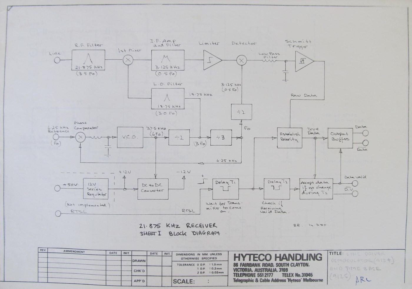
The first drawing here is a block diagram as drawn by Roger.
This block diagram follows the scheme that I had shown last time. Added details are the phase locked
loop that provided all the reference frequencies.
Roger was a little independent of the team. He had his own drawing conventions and as long as these
did not add confusion or ambiguity, I let them stay as they were. Note that Roger has called the
guidepath frequency f0, whereas, I had dubbed it "U" (for unit frequency). He has identified
frequencies in terms of f0 as well as in Hz. The VCO provides the clock for a flyback converter that
Roger used for a negative rail. There had been a convention that analogue electronics ran from plus
and minus 15 volt rails. I think that the Analog Devices multiplier application notes assumed this.
We compromized and used plus and minus 12 volt rails. The block diagram includes an "Establish Polarity"
block. I recall (now that I see this drawing) that we believed that the data signal had a polarity
ambiguity. That is, depending on the dividers in the PLL in the tractor, and the PLL in this receiver,
the data could come out erect or inverted. Fortunately, the message format included a "Front Porch"
in the Mark state, and this could be used to invert the signal if the receiver output was in the wrong
state during the front porch period. This proved to be inadequate thinking as I explained last time
(and as explained again below).
.
.
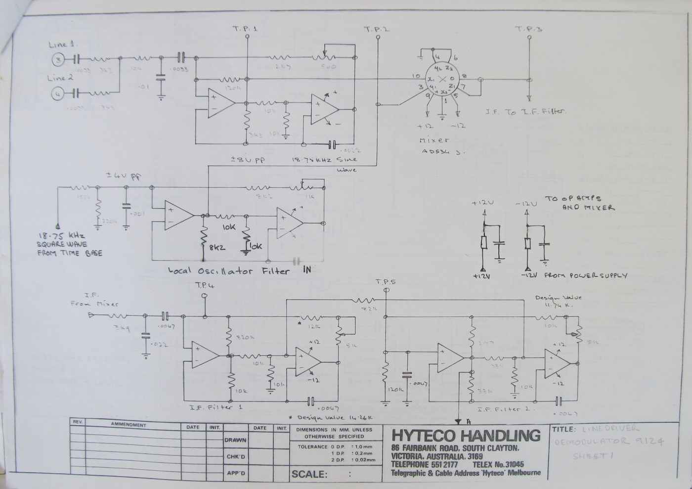
The second drawing is the receiver "Front End".
Note that Roger used a gyrator at the front to pick the carrier out from the guidepath and its harmonics,
instead of the high pass filter in my original plan. The local oscillator (3U, or 3 x f0, or 18.75kHz)
was presented to the mixer as a sinusoidal signal - care of another gyrator. The "IF Strip" along the
bottom of this drawing starts off with capacitor coupling, which, of course, passes no DC, and provides
a very deep notch in the overall receiver pass band at the guidepath 3rd harmonic. There follows two
gyrators to provide a bandpass filter at the IF frequency of 0.5U (3.125kHz). This is a higher performance
IF filter than in my model last time. I had known that my model would work because of the "paper exercise"
that I had done to justify the topology in the first place. Roger had provided extra performance again,
which helps explain the relatively trouble-free testing and debugging phase.
Notice that Roger follows some "old fashioned" drawing conventions. One was to express capacitor values in
microfarads (default), or picofarads. Nanofarads not mentioned. Once apon a time it was always thus.
.
.
The third drawing is the limiter, second mixer (EXOR gate) and trigger and level shifting for following logic.

.
.
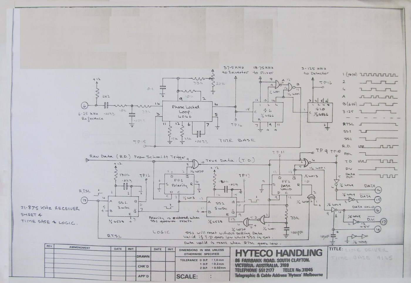
The fourth drawing is the digital stuff. No need for me to go over all of this, as the circuit diagram speaks for itself.
Note that Roger liked to depict logic devices such as a counter or D flip flops, lying on their backs. These were not
the "house conventions", but do not detract from the clarity too much. The one area where I would make the diagram
clearer, is the Phase Locked Loop IC. I am familiar with the 4046 (see
http://www.ti.com/lit/an/scha002a/scha002a.pdf
)
but do not remember all the pin numbers. The components along the bottom of the depiction are the VCO components.
The resistors on pins 11 and 12 and the capacitor between pins 6 and 7 determine the free running frequency and the
frequency range. Roger has used the EXOR gate phase comparitor option (pin 2). The "Loop Filter" (which always
seems so important to me, and which I give much greater prominance) is made up of the resistor between pins 2 and 9
and the capacitor on pin 9. Free running frequency is adjusted by "pulling" the loop filter output with the pot.
Apart from that, his diagram follows good left-to-right practice. Pins 14 and 3 are the phase comparitor inputs,
and pin 4 is the VCO output.
I am a little confused about what supply voltage was used for different parts of the logic. Although not shown, it is
evident that the 4046 PLL IC was run from the 12 volt rail. This can be deduced from the power supply below.
.
.
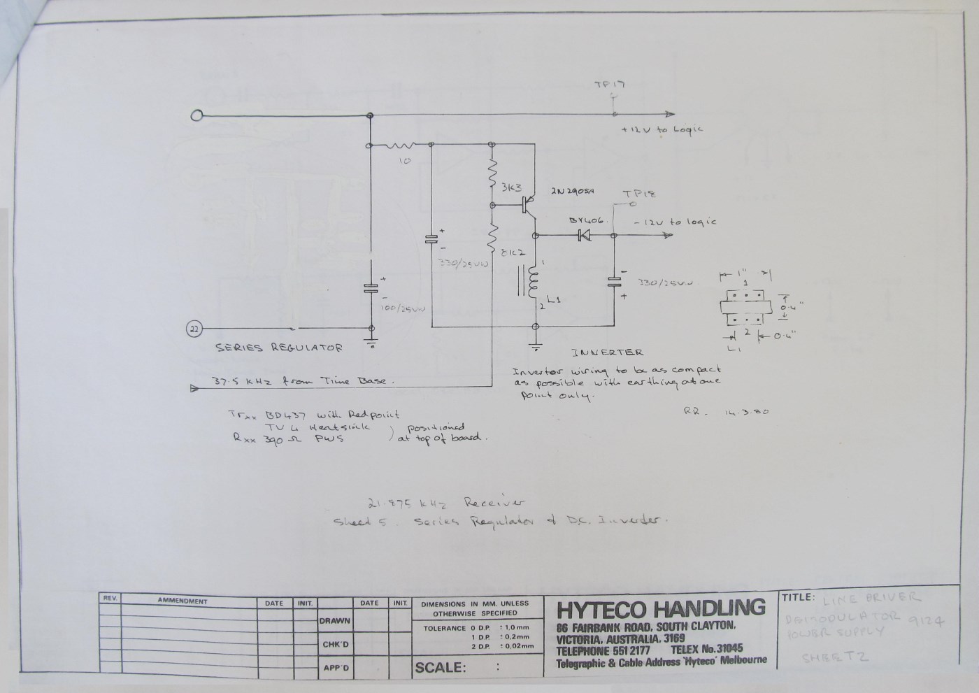
The next page shows the switched mode converter for the minus 12 volts supply. This flyback converter looks very
simple at first glance. It relies on the clock signal from the 4046 having a 50% duty cycle. This has the result
that, (ignoring switch and diode volt drop), the output negative voltage is of the same magnitude as the input
voltage. To achieve this, there must be continuous inductor current. Unfortunately, we do not have an inductance
value, but it would not have been difficult for Roger to choose a suitable value. I have simulated the circuit,
and I find that it is well behaved. I chose 10mH for the inductor. It responds with a well dampled response to a
step change in load current from about 10mA to 20mA. These days, one would probably use a p channel FET instead
of the 2N2905A. How many people would just incorporate a switched mode controller chip without reflecting on
whether it is really necessary?
.
.
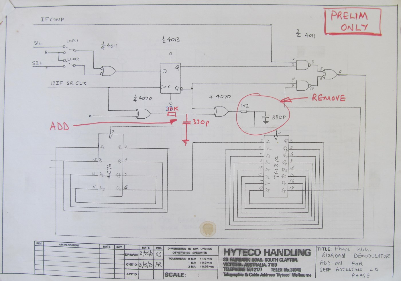
The last sheet is not drawn by Roger: it is drawn by me! This is the add-on to solve the problem of indeterminate
signal phase that I described in the last post. I am glad to see that I had made an apparently last-moment decision
to remove a "slowing down" of the edge of the clock signal to the two registers. The 3/4 of a 4011 in the top right
corner provides a multiplexer. The two registers are wired up as a 12 stage shift register (I might have had the
number of stages wrong in the last posting. It was dictated by the available clock) Up until the start of the message,
the shift register is fed from a signal designated "IF COMP". That signal name does not appear in Roger's circuits,
but it would have been just after the limiter. At the crucial moment during the message "front porch" time, the
D flip flop changes state, and the mux then feeds the shift register input with its own output. From that moment,
whatever waveform was in the shift register is used as the second local oscilator. It represents the phase of the
IF signal that corresponds to a MARK in the data. Obviously, all the 4000 series CMOS can work at 12 volts. I have
just checked, and the 74C374 can as well, so possibly all this logic was running at 12 volts.
Should have been made clear!
Those interested in reading some more about the Riordan Gyrator might like to look at Roger's web page, which is at
http://www.corybas.com/
...but I can't see how to get from there to the pages that I want to refer you to.
So I suggest that you bypass Roger's site's hyperlink system and go directly to one or other of these:
"Career" including VET
http://corybas.com/?ident=10W0L
"Simulated Inductors" (This is the original Gyrator paper.)
http://corybas.com/?ident=10W0G
Also look at this US Patent:
https://www.google.com/patents/US3824496
And this paper:
http://calhoun.nps.edu/bitstream/handle/10945/13161/studyofgyratorci00kule.pdf?sequence=1
Use your browser BACK button to return to the main Blog page.